
Kraklog
[STM32] GPIO Blink ,StandLight 본문
프로그램 : Cube IDE (링크)
사용보드 : STM32 F411 Nucleo 64
지난 과제 : 정해진 GPIO별 다른 속도로 Blink
이걸 하기 위해서
이런식으로 코드를 작성했었다.
같은 형태, 같은 모양, 같은 구조로 반복 되고 있음을 알 수 있다.
그럼 이 코딩을 구조체 형식으로 바꾼다면 어떻게 될 까?
1. GPIO 핀 설정

HAL driver 내부에 선언되어있는 GPIO PIN 이름만 재활용.
#define __IO volatile
#define GPIO_PIN_0   0
#define GPIO_PIN_1   1
#define GPIO_PIN_2   2
#define GPIO_PIN_3   3
#define GPIO_PIN_4   4
#define GPIO_PIN_5   5
#define GPIO_PIN_6   6
#define GPIO_PIN_7   7
#define GPIO_PIN_8   8
#define GPIO_PIN_9   9
#define GPIO_PIN_10  10
#define GPIO_PIN_11  11
#define GPIO_PIN_12  12
#define GPIO_PIN_13  13
#define GPIO_PIN_14  14
#define GPIO_PIN_15  15
기존과 다르게, 핀 번호들을 직접 할당했다.
주소가 아닌 일반 값만 할당되어진 상태이기때문에, 현재 상태로는 사용할 수 없다.
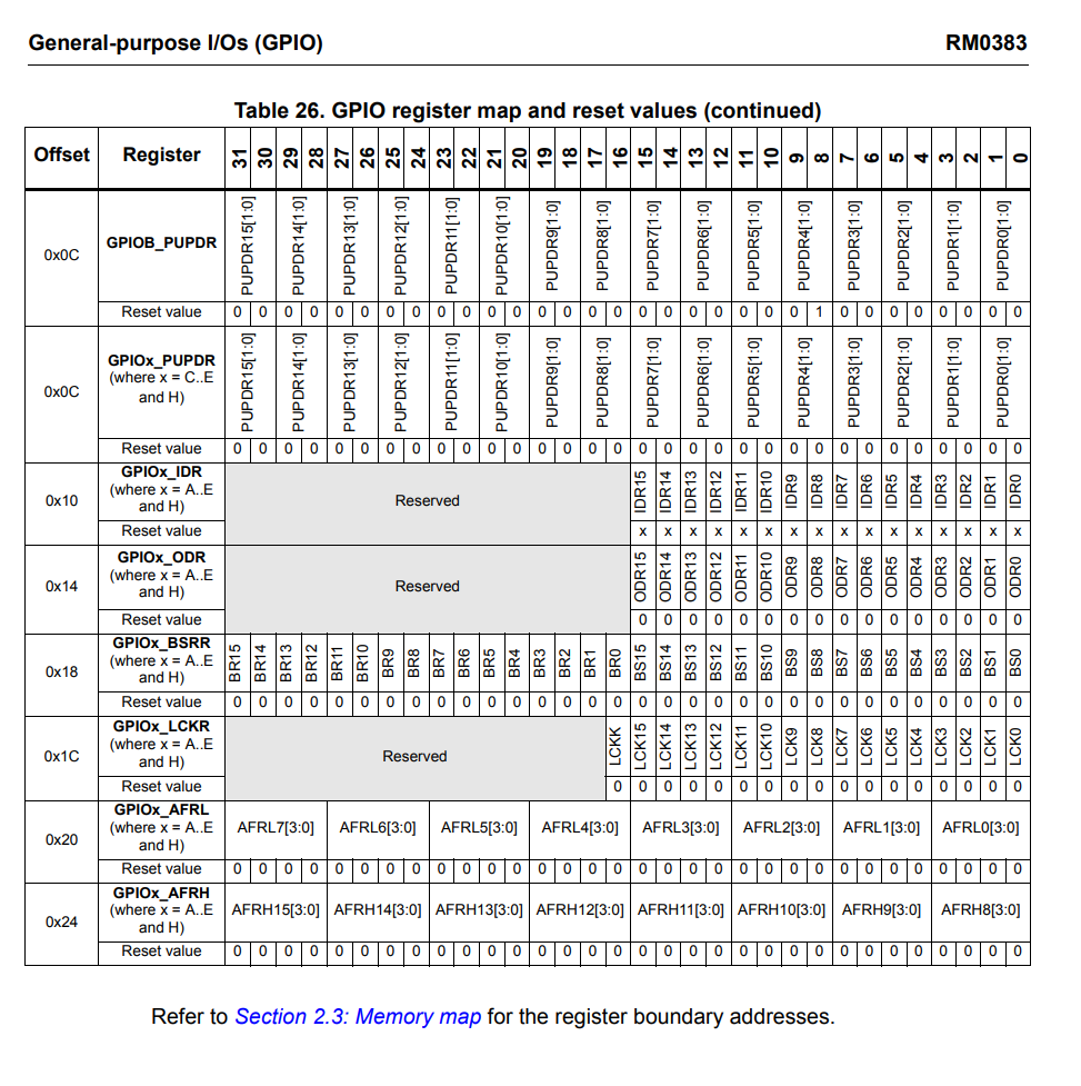
2. Reference menual (GPIO register map) 에 맞춰서 GPIO 타입을 구조체 레지스터를 작성해주었다.

#include <stdint.h>

typedef struct {
	uint32_t MODER;
	uint32_t OTYPER;
	uint32_t OSPEEDR;
	uint32_t IDR;
	uint32_t ODR;
	uint32_t BSRR;
	uint32_t LCKR;
	uint32_t AFRL;
	uint32_t AFRH;
}GPIO_TypeDef;
하지만 이건 그냥 레지스터이기 때문에 volatile을 작성해주어야 한다.
typedef struct {
	volatile uint32_t MODER;
	volatile uint32_t OSPEEDR;
	volatile uint32_t IDR;
	volatile uint32_t OTYPER;
	volatile uint32_t ODR;
	volatile uint32_t BSRR;
	volatile uint32_t LCKR;
	volatile uint32_t AFRL;
	volatile uint32_t AFRH;
}GPIO_TypeDef;
즉, 컴파일에게 최적화를 하지말고, 전부 다 잡으라고 명령한 셈. (레지스터로 빌드할때 volatile을 작성해주는 이유)
#include "stdint.h"

#define __IO volatile
#define GPIO_PIN_0   0
#define GPIO_PIN_1   1
#define GPIO_PIN_2   2
#define GPIO_PIN_3   3
#define GPIO_PIN_4   4
#define GPIO_PIN_5   5
#define GPIO_PIN_6   6
#define GPIO_PIN_7   7
#define GPIO_PIN_8   8
#define GPIO_PIN_9   9
#define GPIO_PIN_10  10
#define GPIO_PIN_11  11
#define GPIO_PIN_12  12
#define GPIO_PIN_13  13
#define GPIO_PIN_14  14
#define GPIO_PIN_15  15

typedef struct {
	volatile uint32_t MODER  ;
	volatile uint32_t OTYPER ;
	volatile uint32_t OSPEEDR;
	volatile uint32_t PUPDR  ;
	volatile uint32_t IDR    ;
	volatile uint32_t ODR    ;
	volatile uint32_t BSRR   ;
	volatile uint32_t LCKR   ;
	volatile uint32_t AFRL   ;
	volatile uint32_t AFRL   ;
}GPIO_TypeDef;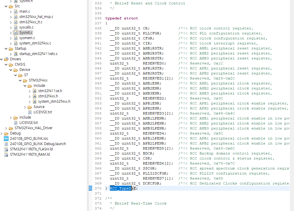
위와 같은 방식으로 RCC_TypeDef 도 선언해준다.
RCC_TPYE 구조체를 만들어서 간결하게 하는 이유
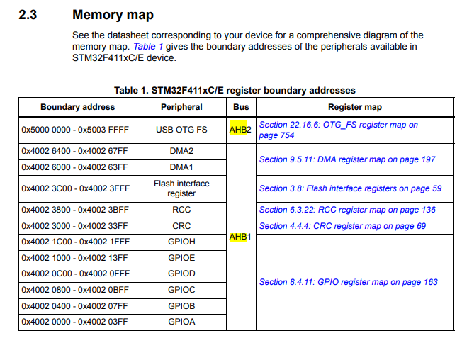
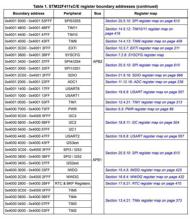
AHB와 APB를 찾아보면 레지스터맵을 확인 할 수 있는데, 주소들이 선언되어있다.
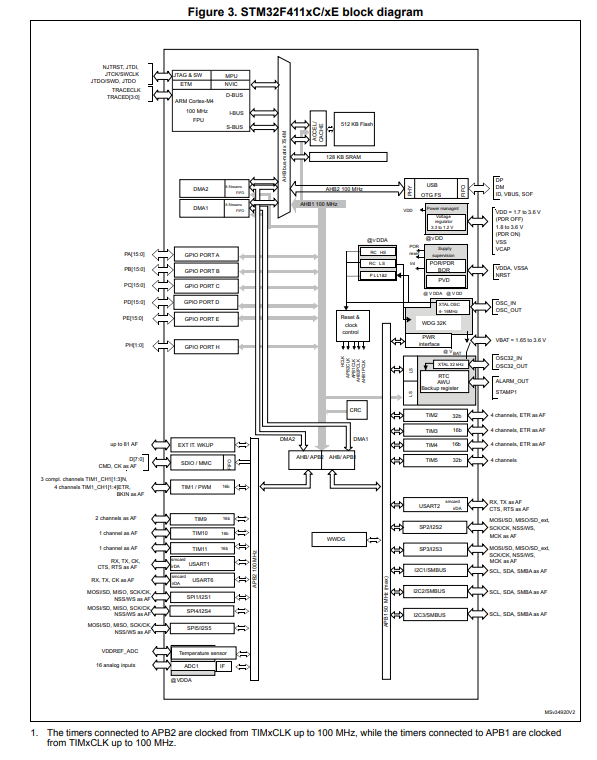
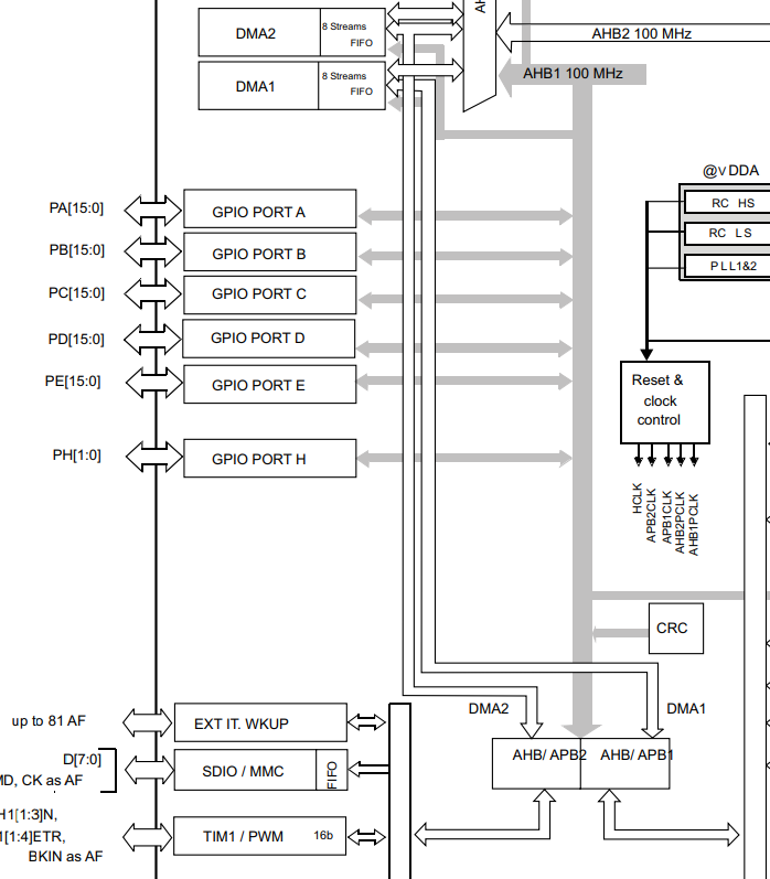
잘 보면, AHB/APB1, AHB/APB2 등등이 이런식으로 연결되어있는데,
구조체를 없이 코드를 작성한다면
#ifndef INC_STM32F411_REG_DEF_H_
#define INC_STM32F411_REG_DEF_H_

#include <stdint.h>

typedef struct {
	volatile uint32_t MODER  ;
	volatile uint32_t OTYPER ;
	volatile uint32_t OSPEEDR;
	volatile uint32_t PUPDR  ;
	volatile uint32_t IDR    ;
	volatile uint32_t ODR    ;
	volatile uint32_t BSRR   ;
	volatile uint32_t LCKR   ;
	volatile uint32_t AFRL   ;
	volatile uint32_t AFRL   ;
}GPIO_TypeDef;

#define RCC_BASE 0x40023800
#define RCC_CR (RCC_BASE + 0x00)
#define RCC_CFGR (RCC_BASE + 0x08)
#define RCC_AHB1 (RCC_BASE + 0x30)


//GPIO_BASE
#define GPIOA_BASE (0x40020000)
#define GPIOB_BASE (0x40020400)
#define GPIOC_BASE (0x40020800)

//GPIO_MODER
#define GPIOA_MODER (GPIOA_BASE + 0x00)
#define GPIOB_MODER (GPIOB_BASE + 0x00)
#define GPIOC_MODER (GPIOC_BASE + 0x00)

//GPIO_OTYPER
#define GPIOA_OTYPER (GPIOA_BASE + 0x04)
#define GPIOB_OTYPER (GPIOB_BASE + 0x04)
#define GPIOC_OTYPER (GPIOC_BASE + 0x04)

//GPIO_OSPEEDR
#define GPIOA_OSPEEDR (GPIOA_BASE + 0x08)
#define GPIOB_OSPEEDR (GPIOB_BASE + 0x08)
#define GPIOC_OSPEEDR (GPIOC_BASE + 0x08)

//GPIO_PUPDR
#define GPIOA_PUPDR (GPIOA_BASE + 0x0C)
#define GPIOB_PUPDR (GPIOB_BASE + 0x0C)
#define GPIOC_PUPDR (GPIOC_BASE + 0x0C)

//GPIO_ODR
#define GPIOA_ODR (GPIOA_BASE +0x14)
#define GPIOB_ODR (GPIOB_BASE +0x14)
#define GPIOC_ODR (GPIOC_BASE +0x14)

#endif /* INC_STM32F411_REG_DEF_H_ */
비슷한 구조의 코드들을 계속해서 반복해서 사용하게 되는데,
#ifndef INC_STM32F411_REG_DEF_H_
#define INC_STM32F411_REG_DEF_H_

#include <stdint.h>

typedef struct {
	volatile uint32_t MODER;
	volatile uint32_t OSPEEDR;
	volatile uint32_t IDR;
	volatile uint32_t OTYPER;
	volatile uint32_t PUPDR;
	volatile uint32_t ODR;
	volatile uint32_t BSRR;
	volatile uint32_t LCKR;
	volatile uint32_t AFRL;
	volatile uint32_t AFRH;
}GPIO_TypeDef;


#define RCC_BASE	0x40023800
#define RCC_CR		(RCC_BASE + 0x00)
#define RCC_CFGR	(RCC_BASE + 0x08)
#define RCC_AHB1	(RCC_BASE + 0x30)


#define GPIOA_BASE (0x40020000)
#define GPIOB_BASE (0x40020400)
#define GPIOC_BASE (0x40020800)

#define GPIOA ((GPIO_TypeDef *)GPIOA_BASE)
#define GPIOB ((GPIO_TypeDef *)GPIOB_BASE)
#define GPIOC ((GPIO_TypeDef *)GPIOC_BASE)


#endif /* INC_STM32F411_REG_DEF_H_ */
이렇게 간결하게 축약시켜줄 수 있다.
#define RCC_BASE 0x40023800
#define RCC_CR (RCC_BASE + 0x00)
#define RCC_CFGR (RCC_BASE + 0x08)
#define RCC_AHB1 (RCC_BASE + 0x30)RCC의 주소를 간소화하는것을 예시로


예시로 3개만 적혀있지만
RCC만해도, 약 20개가 넘어가는데
이런 레지스터 맵을 보면 하나하마다 주소 값을 전부 할당해줘야한다.
(GPIO도 마찬가지)
#include "stdint.h"
#define __IO volatile
#define GPIO_PIN_0 0
#define GPIO_PIN_1 1
#define GPIO_PIN_2 2
#define GPIO_PIN_3 3
#define GPIO_PIN_4 4
#define GPIO_PIN_5 5
#define GPIO_PIN_6 6
#define GPIO_PIN_7 7
#define GPIO_PIN_8 8
#define GPIO_PIN_9 9
#define GPIO_PIN_10 10
#define GPIO_PIN_11 11
#define GPIO_PIN_12 12
#define GPIO_PIN_13 13
#define GPIO_PIN_14 14
#define GPIO_PIN_15 15
typedef struct
{
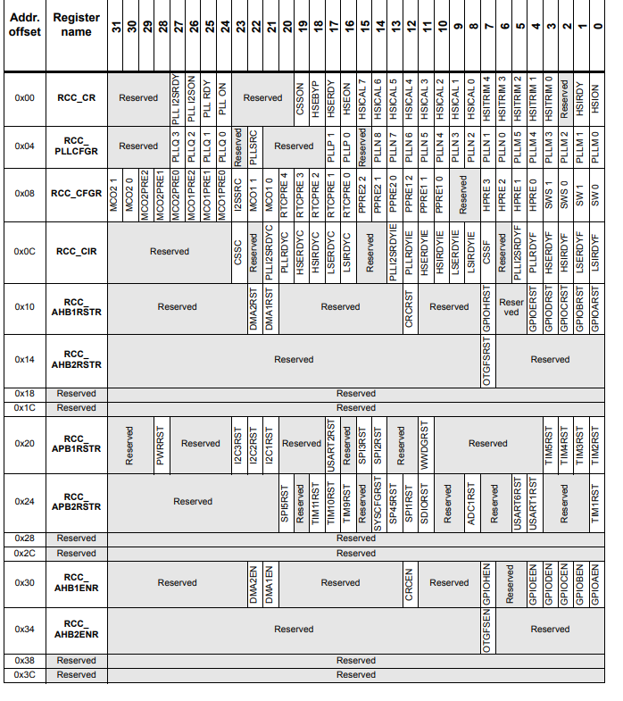
__IO uint32_t CR; /*!< RCC clock control register, Address offset: 0x00 */
__IO uint32_t PLLCFGR; /*!< RCC PLL configuration register, Address offset: 0x04 */
__IO uint32_t CFGR; /*!< RCC clock configuration register, Address offset: 0x08 */
__IO uint32_t CIR; /*!< RCC clock interrupt register, Address offset: 0x0C */
__IO uint32_t AHB1RSTR; /*!< RCC AHB1 peripheral reset register, Address offset: 0x10 */
__IO uint32_t AHB2RSTR; /*!< RCC AHB2 peripheral reset register, Address offset: 0x14 */
__IO uint32_t AHB3RSTR; /*!< RCC AHB3 peripheral reset register, Address offset: 0x18 */
uint32_t RESERVED0; /*!< Reserved, 0x1C */
__IO uint32_t APB1RSTR; /*!< RCC APB1 peripheral reset register, Address offset: 0x20 */
__IO uint32_t APB2RSTR; /*!< RCC APB2 peripheral reset register, Address offset: 0x24 */
uint32_t RESERVED1[2]; /*!< Reserved, 0x28-0x2C */
__IO uint32_t AHB1ENR; /*!< RCC AHB1 peripheral clock register, Address offset: 0x30 */
__IO uint32_t AHB2ENR; /*!< RCC AHB2 peripheral clock register, Address offset: 0x34 */
__IO uint32_t AHB3ENR; /*!< RCC AHB3 peripheral clock register, Address offset: 0x38 */
uint32_t RESERVED2; /*!< Reserved, 0x3C */
__IO uint32_t APB1ENR; /*!< RCC APB1 peripheral clock enable register, Address offset: 0x40 */
__IO uint32_t APB2ENR; /*!< RCC APB2 peripheral clock enable register, Address offset: 0x44 */
uint32_t RESERVED3[2]; /*!< Reserved, 0x48-0x4C */
__IO uint32_t AHB1LPENR; /*!< RCC AHB1 peripheral clock enable in low power mode register, Address offset: 0x50 */
__IO uint32_t AHB2LPENR; /*!< RCC AHB2 peripheral clock enable in low power mode register, Address offset: 0x54 */
__IO uint32_t AHB3LPENR; /*!< RCC AHB3 peripheral clock enable in low power mode register, Address offset: 0x58 */
uint32_t RESERVED4; /*!< Reserved, 0x5C */
__IO uint32_t APB1LPENR; /*!< RCC APB1 peripheral clock enable in low power mode register, Address offset: 0x60 */
__IO uint32_t APB2LPENR; /*!< RCC APB2 peripheral clock enable in low power mode register, Address offset: 0x64 */
uint32_t RESERVED5[2]; /*!< Reserved, 0x68-0x6C */
__IO uint32_t BDCR; /*!< RCC Backup domain control register, Address offset: 0x70 */
__IO uint32_t CSR; /*!< RCC clock control & status register, Address offset: 0x74 */
uint32_t RESERVED6[2]; /*!< Reserved, 0x78-0x7C */
__IO uint32_t SSCGR; /*!< RCC spread spectrum clock generation register, Address offset: 0x80 */
__IO uint32_t PLLI2SCFGR; /*!< RCC PLLI2S configuration register, Address offset: 0x84 */
uint32_t RESERVED7[1]; /*!< Reserved, 0x88 */
__IO uint32_t DCKCFGR; /*!< RCC Dedicated Clocks configuration register, Address offset: 0x8C */
} RCC_TypeDef;
typedef struct {
volatile uint32_t MODER ;
volatile uint32_t OTYPER ;
volatile uint32_t OSPEEDR;
volatile uint32_t PUPDR ;
volatile uint32_t IDR ;
volatile uint32_t ODR ;
volatile uint32_t BSRR ;
volatile uint32_t LCKR ;
volatile uint32_t AFRL ;
volatile uint32_t AFRL ;
}GPIO_TypeDef;
#define RCC_BASE 0x40023800
#define GPIOA_BASE (0x40020000)
#define GPIOB_BASE (0x40020400)
#define GPIOC_BASE (0x40020800)
#define RCC ((RCC_TypeDef *)RCC_BASE)
#define GPIOA ((GPIO_TypeDef *)GPIOA_BASE)
#define GPIOB ((GPIO_TypeDef *)GPIOB_BASE)
#define GPIOC ((GPIO_TypeDef *)GPIOC_BASE)
이제 BASE 주소에 *_TypeDef 에 선언된 헤더가 입력되어진다.
따라서 이젠 이 값을 어떻게 동작해줄지에 대한 동작을 선언해주어야 한다.

- (1 << 1)은 2의 제곱을 의미하므로 2를 나타냅니다.
- (1 << 0)은 1의 제곱을 의미하므로 1을 나타냅니다.
- ((1 << 1) | (1 << 0))는 2번 비트와 1번 비트가 1로 설정된 값을 만듭니다. 따라서 이는 3을 나타냅니다.
- ~는 비트를 뒤집는 연산자이므로, ~((1 << 1) | (1 << 0))은 3의 비트를 뒤집어서 나온 결과인 -4가 됩니다. (~3은 -4입니다.)
- RCC->CFGR &= ~((1 << 1) | (1 << 0))는 현재 RCC 레지스터의 CFGR 필드와 -4를 비트 AND 연산하여, 1번 비트와 0번 비트를 0으로 만듭니다.
이렇게 되면 RCC 레지스터의 CFGR 필드에서 1번 비트와 0번 비트는 0으로 설정되고, 나머지 비트는 변하지 않습니다. 이 작업은 특정 레지스터 필드의 값을 수정하거나 초기화할 때 사용될 수 있습니다.

- (1 << 0)은 1의 제곱을 의미하므로 0번 비트를 1로 설정합니다.
- (1 << 1)은 2의 제곱을 의미하므로 1번 비트를 1로 설정합니다.
- (1 << 2)은 4의 제곱을 의미하므로 2번 비트를 1로 설정합니다.
- ((1 << 0) | (1 << 1) | (1 << 2))는 0번, 1번, 2번 비트가 1로 설정된 값을 만듭니다. 따라서 이 값은 7이 됩니다.
따라서 RCC->AHB1ENR |= ((1 << 0) | (1 << 1) | (1 << 2))는 현재 RCC 레지스터의 AHB1ENR 필드와 7을 비트 OR 연산하여, 0번, 1번, 2번 비트를 1로 설정합니다.
이러한 비트 연산을 사용하여 특정 기능을 활성화하거나 비활성화하는 것은 마이크로컨트롤러의 레지스터 설정에서 흔히 볼 수 있는 패턴 중 하나입니다.
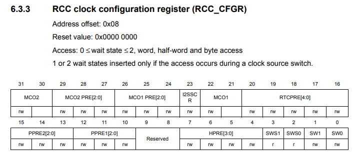
우선 ChatGPT를 이용한 해설이긴하나,
Reference Menual을 통해서 레지스터를 어떻게 맵핑에 따라 작동할지를 작성해준다.
void Sysinit()
{
//RCC_CR
//0x40023800 |= (1<<0); incorrect, bec 0x40023800 it is not address, constant. need casting
//(unsigned long *)0x40023800 |= (1<<0); //(unsinged long *) means it is address, long
(uint32_t *)0x40023800 |= (1<<0); //(uint32_t *) means it is address, usigned int 32bit , 0번에 있는 값만 1로 shift하겠다 (|= (1<<0) )
*(uint32_t *)RCC_CFGR &= ~(1<<0);
*(uint32_t *)RCC_CFGR &= ~(1<<1);
*(uint32_t *)RCC_CFGR &= ~((1<<1)|(1<<0)); //HSI Selected
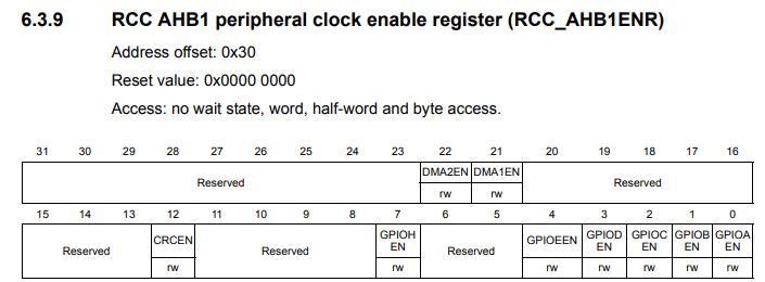
*(uint32_t *)RCC_AHB1 |= (1<<0); // GPIOA clock enable
*(uint32_t *)RCC_AHB1 |= (1<<1); // GPIOA clock enable
*(uint32_t *)RCC_AHB1 |= (1<<2); // GPIOA clock enable
*(uint32_t *)RCC_CR =*(uint32_t *)RCC_CR (1<<0); //*(type *)address constant
*(uint32_t *)RCC_CR |= (1<<0); // HSI ON
RCC -> CFGR &= ~((1<<1)|(1<<0));
RCC -> AHB1ENR |= ((1<<0)|(1<<1)|(1<<2)); // GPIOA,B,C clock enable
RCC -> CR |= (1<<0);
/////GPIOA///////
GPIOA -> MODER |=(1<<10);//GPIOA 5pin output mode.
GPIOA -> OTYPER &=~(1<<5);//GPIOA 5pin push-pull.
GPIOA -> OSPEEDR |=(1<<11)|(1<<10);//GPIOA 5pin high speed.
GPIOA -> PUPDR |=(1<<10); //GPIOA 5pin pull-up
GPIOA -> MODER |=(1<<24);//GPIOA 12pin output mode.
GPIOA -> OTYPER &=~(1<<12);//GPIOA 12pin push-pull.
GPIOA -> OSPEEDR |=(1<<25)|(1<<24);//GPIOA 12pin high speed.
GPIOA -> PUPDR |=(1<<24); //GPIOA 12pin pull-up
////GPIOB////
GPIOB -> MODER |=(1<<2); //GPIOA 5pin output mode.
GPIOB -> OTYPER &=~(1<<1);//GPIOB 1pin push-pull.
GPIOB -> OSPEEDR |=(1<<3)|(1<<2);//GPIOB 1pin high speed.
GPIOB -> PUPDR |=(1<<2); //GPIOB 1pin pull-up
////GPIOC////
GPIOC -> MODER |=(1<<16); //GPIOC pin output mode.
GPIOC -> OTYPER &=~(1<<8);//GPIOB /pin push-pull.
GPIOC -> OSPEEDR |=(1<<17)|(1<<16);//GPIOB 8pin high speed.
GPIOC -> PUPDR |=(1<<16); //GPIOB 8pin pull-up
GPIOC->MODER &= ~((1<<9)|(1<<8)); // GPIOC 4pin output mode
GPIOC->PUPDR |= (1<<8); // GPIOC 4pin pull-up
}void Sysinit(){
RCC -> CFGR &= ~((1<<1)|(1<<0));
RCC -> AHB1ENR |= ((1<<0)|(1<<1)|(1<<2)); //GPIO A B C CLOCK ENB
RCC -> CR |= (1<<0);
//////////GPIOA PIN//////////
GPIOA -> MODER |=(1<<10);//GPIOA 5pin output mode.
GPIOA -> OTYPER &=~(1<<5);//GPIOA 5pin push-pull.
GPIOA -> OSPEEDR |=(1<<11)|(1<<10);//GPIOA 5pin high speed.
GPIOA -> PUPDR |=(1<<10); //GPIOA 5pin pull-up
GPIOA -> MODER |=(1<<24);//GPIOA 12pin output mode.
GPIOA -> OTYPER &=~(1<<12);//GPIOA 12pin push-pull.
GPIOA -> OSPEEDR |=(1<<25)|(1<<24);//GPIOA 12pin high speed.
GPIOA -> PUPDR |=(1<<24); //GPIOA 12pin pull-up
//////////GPIOB PIN//////////
GPIOB -> MODER |=(1<<2); //GPIOA 5pin output mode.
GPIOB -> OTYPER &=~(1<<1);//GPIOB 1pin push-pull.
GPIOB -> OSPEEDR |=(1<<3)|(1<<2);//GPIOB 1pin high speed.
GPIOB -> PUPDR |=(1<<2); //GPIOB 1pin pull-up
//////////GPIOC PIN//////////
GPIOC -> MODER |=(1<<16); //GPIOC pin output mode.
GPIOC -> OTYPER &=~(1<<8);//GPIOC /pin push-pull.
GPIOC -> OSPEEDR |=(1<<17)|(1<<16);//GPIOB 8pin high speed.
GPIOC -> PUPDR |=(1<<16); //GPIOC 8pin pull-up
GPIOC->MODER &= ~((1<<9)|(1<<8)); // GPIOC 4pin output mode
GPIOC->PUPDR |= (1<<8); // GPIOC 4pin pull-up
}이렇게 적용시킬 수 있다.
/*
 * SysInit.c
 *
 *  Created on: Jan 8, 2024
 *      Author: kccistc
 */
#include <stdint.h>
#include <STM32F411_Reg_Def.h>


void Sysinit()
{
   //RCC_CR
   //0x40023800 |= (1<<0); incorrect, bec 0x40023800 it is not address, constant. need casting
   //(unsigned long *)0x40023800 |= (1<<0); //(unsinged long *) means it is address, long
   //(uint32_t *)0x40023800 |= (1<<0); //(uint32_t *) means it is address, usigned int 32bit , 0번에 있는 값만 1로 shift하겠다 (|= (1<<0) )


   //*(uint32_t *)RCC_CFGR &= ~(1<<0);
   //*(uint32_t *)RCC_CFGR &= ~(1<<1);
   *(uint32_t *)RCC_CFGR &= ~((1<<1)|(1<<0));  //HSI Selected
   *(uint32_t *)RCC_AHB1 |= (1<<0); // GPIOA clock enable
   *(uint32_t *)RCC_AHB1 |= (1<<1); // GPIOA clock enable
   *(uint32_t *)RCC_AHB1 |= (1<<2); // GPIOA clock enable

   //*(uint32_t *)RCC_CR =*(uint32_t *)RCC_CR (1<<0); //*(type *)address constant
   *(uint32_t *)RCC_CR |= (1<<0); // HSI ON


   *(uint32_t*) GPIOA_MODER |=(1<<10); //GPIOA 5pin output mode.
   *(uint32_t*) GPIOA_MODER |=(1<<24); //GPIOA 12pin output mode.
   *(uint32_t*) GPIOA_OTYPER &=~(1<<5);//GPIOA 5pin push-pull.
   *(uint32_t*) GPIOA_OTYPER &=~(1<<12);//GPIOA 12pin push-pull.
   *(uint32_t*) GPIOA_OSPEEDR |=(1<<11)|(1<<10);//GPIOA 5pin high speed.
   *(uint32_t*) GPIOA_OSPEEDR |=(1<<25)|(1<<24);//GPIOA 12pin high speed.
   *(uint32_t*) GPIOA_PUPDR |=(1<<10); //GPIOA 5pin pull-up
   *(uint32_t*) GPIOA_PUPDR |=(1<<24); //GPIOA 12pin pull-up


   *(uint32_t*) GPIOB_MODER |=(1<<2); //GPIOA 5pin output mode.
   *(uint32_t*) GPIOB_OTYPER &=~(1<<1);//GPIOB 1pin push-pull.
   *(uint32_t*) GPIOB_OSPEEDR |=(1<<3)|(1<<2);//GPIOB 1pin high speed.
   *(uint32_t*) GPIOB_PUPDR |=(1<<2); //GPIOB 1pin pull-up

   *(uint32_t*) GPIOC_MODER |=(1<<16); //GPIOA 5pin output mode.
   *(uint32_t*) GPIOC_OTYPER &=~(1<<8);//GPIOB 1pin push-pull.
   *(uint32_t*) GPIOC_OSPEEDR |=(1<<17)|(1<<16);//GPIOB 1pin high speed.
   *(uint32_t*) GPIOC_PUPDR |=(1<<16); //GPIOB 1pin pull-up


}

void delay(uint32_t ms)
{
   uint32_t temp = ms * 1000;

   while(temp) temp--; //0이 될때까지...
}
delay 함수를 사용하기위해서 delay 함수까지 선언
3.코드 작성

SW를 작성하기위해서는 이런식으로 Layer를 나눠줘야한다.
HAL 드라이버를 사용하는 이유는 예를들어 개발은 F411을 사용했으나, F103으로 바꿔야 하는 경우 라던가
개발을 혼자서 전체적으로 하지 않고, 파트별로 나눠서 하는 경우, 수정과 통합의 용이성이 있기 때문이다.
즉, 유지보수가 더 쉬워진다는 장점을 갖게 된다.


main 함수가 light함수를 call 하고 있다. (main이 caller ,lightwrite가 callee)
결국 GPIOA->ODR |= (1<<12); GPIOA->ODR &= ~(1<<12); 를 간단화 시켰다.
이를 "추상화" 시켰다고한다. (추상화 : 복잡한것을 Simple하게 만들었다)
main 함수란 무엇일까?
1. 초기화를 해주는 것.
2. Application 의 시동, 시작을 나타내는 함수
-학부시절에 여기에 모든 내용을 적었었는데, 정확하게 프로그래밍을 하기위해서는 동작 내용은 따로 빼내주는것이 좋다.


main.c에 있던 내용을 옮겨주고
헤더 작업을 해준다. (light.c에 정의해준 Light on은 light.h로 옮겨주었다. light.h를 선언해주었기 때문에)

현재 코드는 STM32에 결합력이 강한 상태이다.
실제로 개발을하고, 업데이트 혹은 상용화 과정을 하면서 칩셋등이 바뀌게되는 경우도 있는데
이런식으로 코딩이 되어있다면, 칩을 바꾸거나 업데이트를 하는 등의 이유때마다 모든 코드를 수정하게 되는 경우가 생길 수 있다.
위와 같은 컨셉으로 만들 예정.

/*
 * Led.c
 *
 *  Created on: Jan 9, 2024
 *      Author: kccistc
 */

#ifndef DRIVER_LED_LED_C_
#define DRIVER_LED_LED_C_

#include "Led.h"
#include "stdint.h"

void LedOn(uint32_t ledNum)
{
	switch(ledNum)
	{
	case 0:
		LED_1_GPIO_PORT ->ODR |= (1<<LED_1_GPIO_PIN);
		break;
	case 1:
		LED_2_GPIO_PORT->ODR |= (1<<LED_2_GPIO_PIN);
		break;
	case 2:
		LED_3_GPIO_PORT->ODR |= (1<<LED_3_GPIO_PIN);
		break;
	default :
		LED_1_GPIO_PORT->ODR |= (1<<LED_1_GPIO_PIN);
		}
}

void LedOff(uint32_t ledNum)
{
	switch(ledNum)
		{
		case 0:
			LED_1_GPIO_PORT->ODR &= ~(1<<LED_1_GPIO_PIN);
			break;
		case 1:
			LED_2_GPIO_PORT->ODR &= ~(1<<LED_2_GPIO_PIN);
			break;
		case 2:
			LED_2_GPIO_PORT->ODR &= ~(1<<LED_3_GPIO_PIN);
			break;
		default :
			LED_1_GPIO_PORT->ODR &=~(1<<LED_1_GPIO_PIN);
			}
}


#endif /* DRIVER_LED_LED_C_ */
/*
* Led.h
*
* Created on: Jan 9, 2024
* Author: kccistc
*/
#ifndef DRIVER_LED_LED_H_
#define DRIVER_LED_LED_H_
#include "stdint.h"
#include "../../Inc/STM32F411_Reg_Def.h"
#define LED_1_GPIO_PORT GPIOA
#define LED_2_GPIO_PORT GPIOB
#define LED_3_GPIO_PORT GPIOC
#define LED_1_GPIO_PIN GPIO_PIN_5
#define LED_2_GPIO_PIN GPIO_PIN_1
#define LED_3_GPIO_PIN GPIO_PIN_8
void LedOn(uint32_t ledNum);
void LedOff(uint32_t ledNum);
#endif /* DRIVER_LED_LED_H_ */
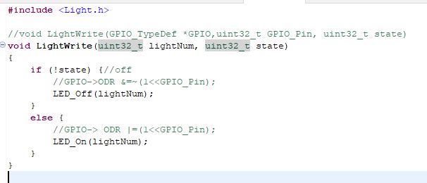
//light.c
#include "Light.h"
//void LightWrite(GPIO_TypeDef *GPIO,uint32_t GPIO_Pin, uint32_t state)
void LightWrite(uint32_t lightNum, uint32_t state)
{
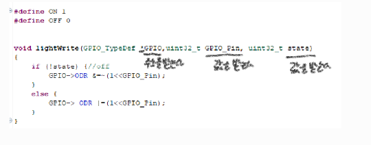
if (!state) {//off
//GPIO->ODR &=~(1<<GPIO_Pin);
LedOff(lightNum);
}
else {
//GPIO-> ODR |=(1<<GPIO_Pin);
LedOn(lightNum);
}
}//Light.c
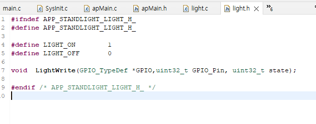
#ifndef APP_STANDLIGHT_LIGHT_H_
#define APP_STANDLIGHT_LIGHT_H_
#include <stdint.h>
#include "../../driver/Led/Led.h"
#define LIGHT_ON 1
#define LIGHT_OFF 0
#define LIGHT_0 0
#define LIGHT_1 1
#define LIGHT_2 2
//void LightWrite(GPIO_TypeDef *GPIO,uint32_t GPIO_Pin, uint32_t state);
void LightWrite(uint32_t lightNum, uint32_t state);
#endif /* APP_STANDLIGHT_LIGHT_H_ */
/*
 * apMain.c
 *
 *  Created on: Jan 9, 2024
 *      Author: kccistc
 */


#include "apMain.h"

void apMain()
{
	while(1)
	{
		LightWrite(LIGHT_0,LIGHT_ON);
		LightWrite(LIGHT_1,LIGHT_ON);
		LightWrite(LIGHT_2,LIGHT_ON);
		delay(500);
		LightWrite(LIGHT_0,LIGHT_OFF);
		LightWrite(LIGHT_1,LIGHT_OFF);
		LightWrite(LIGHT_2,LIGHT_OFF);

		delay(500);
	}
}
/*
* apMain.h
*
* Created on: Jan 9, 2024
* Author: kccistc
*/
#ifndef APP_APMAIN_H_
#define APP_APMAIN_H_
#include "Standlight/Light.h"
#endif /* APP_APMAIN_H_ */#ifndef INC_STM32F411_REG_DEF_H_
#define INC_STM32F411_REG_DEF_H_
#define RCC_BASE 0x40023800
#define RCC_CR (RCC_BASE + 0x00)
#define RCC_CFGR (RCC_BASE + 0x08)
#define RCC_AHB1 (RCC_BASE + 0x30)
//GPIO_BASE
#define GPIOA_BASE (0x40020000)
#define GPIOB_BASE (0x40020400)
#define GPIOC_BASE (0x40020800)
//GPIO_MODER
#define GPIOA_MODER (GPIOA_BASE + 0x00)
#define GPIOB_MODER (GPIOB_BASE + 0x00)
#define GPIOC_MODER (GPIOC_BASE + 0x00)
//GPIO_OTYPER
#define GPIOA_OTYPER (GPIOA_BASE + 0x04)
#define GPIOB_OTYPER (GPIOB_BASE + 0x04)
#define GPIOC_OTYPER (GPIOC_BASE + 0x04)
//GPIO_OSPEEDR
#define GPIOA_OSPEEDR (GPIOA_BASE + 0x08)
#define GPIOB_OSPEEDR (GPIOB_BASE + 0x08)
#define GPIOC_OSPEEDR (GPIOC_BASE + 0x08)
//GPIO_PUPDR
#define GPIOA_PUPDR (GPIOA_BASE + 0x0C)
#define GPIOB_PUPDR (GPIOB_BASE + 0x0C)
#define GPIOC_PUPDR (GPIOC_BASE + 0x0C)
//GPIO_ODR
#define GPIOA_ODR (GPIOA_BASE +0x14)
#define GPIOB_ODR (GPIOB_BASE +0x14)
#define GPIOC_ODR (GPIOC_BASE +0x14)/*
* STM32F411_Reg_Def.h
*
* Created on: Jan 8, 2024
* Author: kccistc
*/
#ifndef INC_STM32F411_REG_DEF_H_
#define INC_STM32F411_REG_DEF_H_
#include <stdint.h>
#define __IO volatile
#define GPIO_PIN_0 0
#define GPIO_PIN_1 1
#define GPIO_PIN_2 2
#define GPIO_PIN_3 3
#define GPIO_PIN_4 4
#define GPIO_PIN_5 5
#define GPIO_PIN_6 6
#define GPIO_PIN_7 7
#define GPIO_PIN_8 8
#define GPIO_PIN_9 9
#define GPIO_PIN_10 10
#define GPIO_PIN_11 11
#define GPIO_PIN_12 12
#define GPIO_PIN_13 13
#define GPIO_PIN_14 14
#define GPIO_PIN_15 15
typedef struct
{
__IO uint32_t CR; /*!< RCC clock control register, Address offset: 0x00 */
__IO uint32_t PLLCFGR; /*!< RCC PLL configuration register, Address offset: 0x04 */
__IO uint32_t CFGR; /*!< RCC clock configuration register, Address offset: 0x08 */
__IO uint32_t CIR; /*!< RCC clock interrupt register, Address offset: 0x0C */
__IO uint32_t AHB1RSTR; /*!< RCC AHB1 peripheral reset register, Address offset: 0x10 */
__IO uint32_t AHB2RSTR; /*!< RCC AHB2 peripheral reset register, Address offset: 0x14 */
__IO uint32_t AHB3RSTR; /*!< RCC AHB3 peripheral reset register, Address offset: 0x18 */
uint32_t RESERVED0; /*!< Reserved, 0x1C */
__IO uint32_t APB1RSTR; /*!< RCC APB1 peripheral reset register, Address offset: 0x20 */
__IO uint32_t APB2RSTR; /*!< RCC APB2 peripheral reset register, Address offset: 0x24 */
uint32_t RESERVED1[2]; /*!< Reserved, 0x28-0x2C */
__IO uint32_t AHB1ENR; /*!< RCC AHB1 peripheral clock register, Address offset: 0x30 */
__IO uint32_t AHB2ENR; /*!< RCC AHB2 peripheral clock register, Address offset: 0x34 */
__IO uint32_t AHB3ENR; /*!< RCC AHB3 peripheral clock register, Address offset: 0x38 */
uint32_t RESERVED2; /*!< Reserved, 0x3C */
__IO uint32_t APB1ENR; /*!< RCC APB1 peripheral clock enable register, Address offset: 0x40 */
__IO uint32_t APB2ENR; /*!< RCC APB2 peripheral clock enable register, Address offset: 0x44 */
uint32_t RESERVED3[2]; /*!< Reserved, 0x48-0x4C */
__IO uint32_t AHB1LPENR; /*!< RCC AHB1 peripheral clock enable in low power mode register, Address offset: 0x50 */
__IO uint32_t AHB2LPENR; /*!< RCC AHB2 peripheral clock enable in low power mode register, Address offset: 0x54 */
__IO uint32_t AHB3LPENR; /*!< RCC AHB3 peripheral clock enable in low power mode register, Address offset: 0x58 */
uint32_t RESERVED4; /*!< Reserved, 0x5C */
__IO uint32_t APB1LPENR; /*!< RCC APB1 peripheral clock enable in low power mode register, Address offset: 0x60 */
__IO uint32_t APB2LPENR; /*!< RCC APB2 peripheral clock enable in low power mode register, Address offset: 0x64 */
uint32_t RESERVED5[2]; /*!< Reserved, 0x68-0x6C */
__IO uint32_t BDCR; /*!< RCC Backup domain control register, Address offset: 0x70 */
__IO uint32_t CSR; /*!< RCC clock control & status register, Address offset: 0x74 */
uint32_t RESERVED6[2]; /*!< Reserved, 0x78-0x7C */
__IO uint32_t SSCGR; /*!< RCC spread spectrum clock generation register, Address offset: 0x80 */
__IO uint32_t PLLI2SCFGR; /*!< RCC PLLI2S configuration register, Address offset: 0x84 */
uint32_t RESERVED7[1]; /*!< Reserved, 0x88 */
__IO uint32_t DCKCFGR; /*!< RCC Dedicated Clocks configuration register, Address offset: 0x8C */
} RCC_TypeDef;
typedef struct {
volatile uint32_t MODER ;
volatile uint32_t OTYPER ;
volatile uint32_t OSPEEDR ;
volatile uint32_t PUPDR ;
volatile uint32_t IDR ;
volatile uint32_t ODR ;
volatile uint32_t BSRR ;
volatile uint32_t LCKR ;
volatile uint32_t AFRL ;
volatile uint32_t AFRH ;
}GPIO_TypeDef;
#define RCC_BASE 0x40023800
#define GPIOA_BASE (0x40020000)
#define GPIOB_BASE (0x40020400)
#define GPIOC_BASE (0x40020800)
#define RCC ((RCC_TypeDef *)RCC_BASE)
#define GPIOA ((GPIO_TypeDef *)GPIOA_BASE)
#define GPIOB ((GPIO_TypeDef *)GPIOB_BASE)
#define GPIOC ((GPIO_TypeDef *)GPIOC_BASE)
#endif /* INC_STM32F411_REG_DEF_H_ */
/*
 * Sysinit.h
 *
 *  Created on: Jan 8, 2024
 *      Author: kccistc
 */

#include <stdint.h>
#include <STM32F411_Reg_Def.h>


#ifndef INC_SYSINIT_H_
#define INC_SYSINIT_H_

void Sysinit();
void delay(uint32_t ms);

#endif /* INC_SYSINIT_H_ */
#include <stdint.h>
#include <STM32F411_Reg_Def.h>
#include <SysInit.h>

int main()
{
	Sysinit();

	while(1)
	{
		apMain();
	}

	return 0;
}'[Harman] 하만 반도체 설계 > STM32' 카테고리의 다른 글
| [STM32] LED_Blink (0) | 2024.01.08 |
|---|
